Research and Development Capabilities | Quantiam Technologies Inc.

R&D and Trial Manufacturing Facility

Quantiam’s 34,000-ft2 R&D and trial manufacturing facility in Edmonton houses our extensive in-house materials characterization and development capabilities.  Contact us today to find out how we can solve your materials and process-related pain points.

Materials Characterization

Surface and Advanced Structure Probes

  • Two X-ray diffraction units, one for high temperature
  • One FESEM-EDS and one SEM/EDS
  • Auger Electron Spectroscopy (AES) with SIMS
  • Small-spot X-Ray Photoelectron Spectroscopy (XPS)

Metallography

  • Conventional and Damage-sensitive materials
  • Hot and cold sample mounting
  • Optical microscopy

Physical and Mechanical Properties

  • Hardness testing (micro and macro)
  • Instron Tensile and bend-testing
  • Fracture toughness (pull and bend-testing)
  • Surface roughness and  optical profilometry
  • 3D laser mapping for internal surfaces of tubulars

Particle/Powder Testing

  • Particle size analysis (laser diffraction and DLS)
  • Zeta potential
  • BET surface area

Thermogravimetric Analysis

  • Three TGA units; powder and coupon samples to 35g
  • Up to 1600°C
  • Testing atmospheres include:
    • up to 100% Hydrogen
    • up to 90% steam/humidity
    • Ethane-steam pyrolysis
    • Oxidizing/inert/reducing/reactive gases
  • Differential scanning calorimetry

Electrochemical Testing

  • Keithley single channel potentiostat
  • PARStat 8-channel potentiostat
  • Arbin 32-channel potentiostat with Gamry EIS

Photovoltaic Testing

  • G2V AM1.5G solar simulators
    • 400 cm2
    • 1 m2

Materials Performance Testing

High Temperature Testing

Extensive high temperature testing up to 1500°C under various atmospheres including:

  • Vacuum (< 10-3 Torr)
  • Inert
  • Oxidizing
  • Reducing
  • Carburizing
  • Reactive gases

Wear Performance Testing

  • ASTM G65 Abrasion Wear Testing
  • ASTM G99 Pin-on-Disk Wear Testing
  • ASTM G133 Sliding Wear Testing
  • ASTM G171 Scratch Resistance Testing

Catalyst Testing

Catalyst performance testing/screening:

  • temperatures up to 1000°C
  • pressures up to 50 atm.
  • on-line analysis of reaction products with gas chromatography (GC) and mass spectrometry (MS)


Materials, Manufacturing & Process Development

Rapid Prototyping

  • OpenFoam CAD
  • 3D printing

Coating Development

  • Quantiam-proprietary coating manufacturing technology for internal and external surfaces of complex shapes.
  • tape-casting to 25mm thickness
  • spray coating:
    • 2D Sono-tek spray coater with temperature control
    • 3D 5-axis robot arm spray coater for full-scale workpieces

Powder Processing

  • Ball-milling
  • Mechanical alloying
  • Lab-scale and production-scale attritors

Chemical Process Development

  • Air-free chemical synthesis
  • Modular jacketed reactor system for batch sizes of 100 mL – 5L


Surface Analysis Capabilities

Technique Characteristics
JEOL JSM-7001F FE-SEM/EDS
JEOL JSM-6010LV SEM/EDS
Perkin Elmers PHI-5600 small spot XPS
Perkin Elmers PHI-600 SAM/SIMS
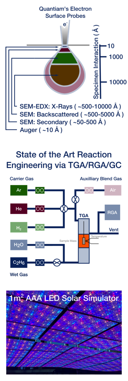
Field Emission Scanning Electron Microscopy w/ Energy Dispersive Spectroscopy Scanning Electron Microscopy w/ Energy Dispersive Spectroscopy X-ray Photoelectron Spectroscopy (XPS) Auger Electron Spectroscopy/Scanning Auger Multiprobe (AES-SAM) Secondary Ion Mass Spectrometry (SIMS)
Probe electrons electrons x-ray electrons ions
Detected Particles electrons and photons electrons and photons electrons electrons +ve or -ve ions
Range B and higher B and higher Li and higher Li and higher 1 - 511 amu
Sampling Depth 0.5 – 5 μm 0.5 – 5 μm 10 - 50 Å 4 - 30 Å 20 - 50 Å
Detection Limit* 0.5 to 2.0 at% 0.5 to 2.0 at% 0.1 to 1.0 at% 0.1 to 1.0 at% ppm to ppb
Depth Profiling (Speed and Type) N/A N/A fast, argon ions fast, argon ions fast, argon/oxygen
Information elemental elemental elemental, chemical elemental, some chemical elemental, some structural
Quantitative semi semi semi semi not usually
Probe Spatial Resolution 1.2 nm 4.0 nm 75 μm ~35 nm 200 μm to 1 mm
Advantages
excellent spatial resolution
elemental mapping
excellent spatial resolution
elemental mapping
few limitations on sample type
chemical state information
low damage to sample
good spatial resolution
elemental mapping
analyzing conductors and semiconductors
excellent sensitivity
isotope and hydrogen detection

* Detection limit varies by element